Set up the physical board
Define the board outline, stack, layers, units, origins, and net classes before detailed placement and routing.
- Board geometry
- Layer stack
- Net classes and constraints
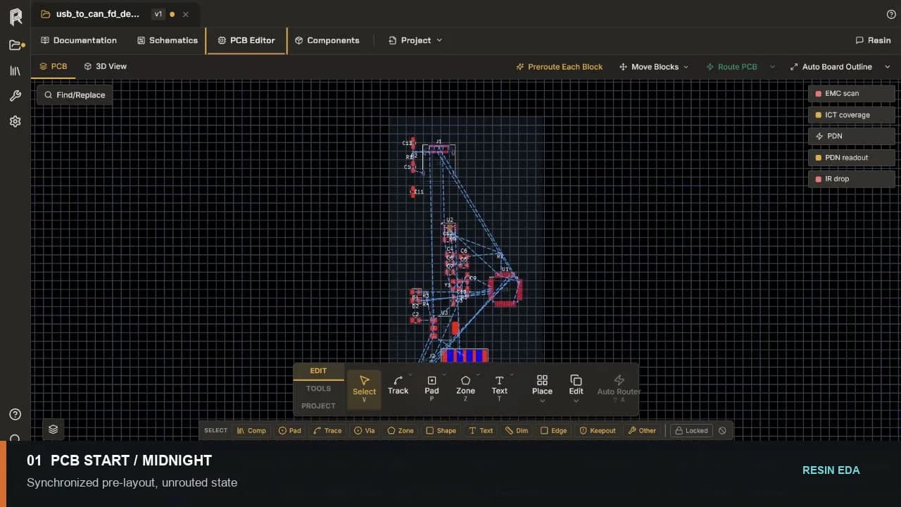
PCB design
Move from synchronized footprints and nets to board geometry, placement, routing, copper zones, design checks, and 3D inspection in one PCB workspace.
No credit card required.
Core capabilities
Define the board outline, stack, layers, units, origins, and net classes before detailed placement and routing.
Position and rotate footprints around connectors, keepouts, fixed interfaces, and the mechanical envelope.
Create and reshape copper with direct control over nets, widths, layers, vias, and zones.
Measure critical relationships, investigate rule findings, and use the 3D view to catch obvious model, orientation, and enclosure problems before release.
Resin EDA
Open the schematic and PCB workspace in your browser. No credit card required.
Questions about team access, security review, or purchasing? Write to hello@resineda.com.