Define the circuit with AI Designer
Explore requirements, architecture, interfaces, parts, and datasheets, then review the proposed work in the editable schematic.
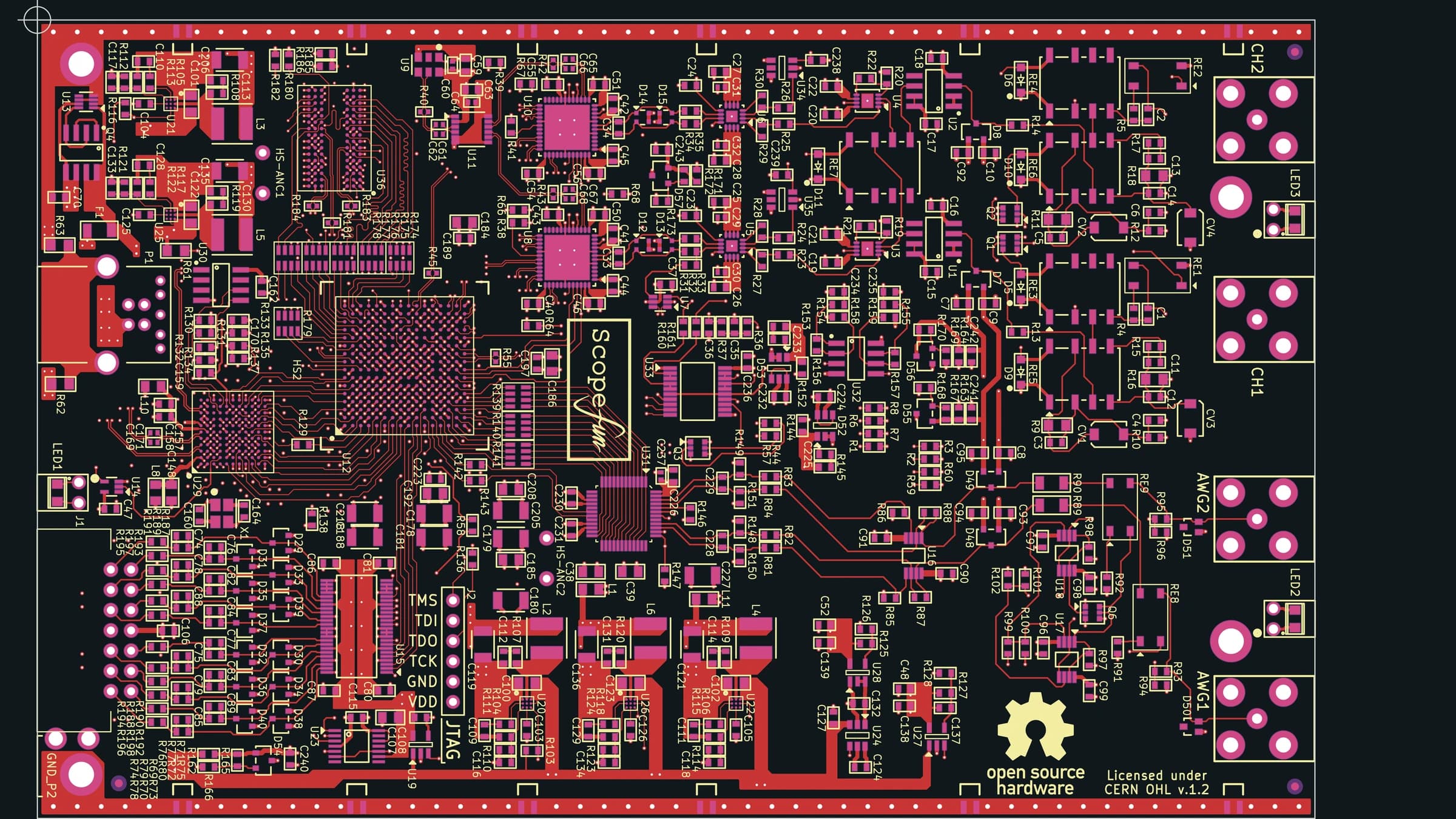
New PCB design
Use AI Designer where it helps, keep direct control in the schematic and PCB editors, run AI Review with ERC and DRC, and finish with an inspected manufacturing package.
No credit card required.
Workflow
Explore requirements, architecture, interfaces, parts, and datasheets, then review the proposed work in the editable schematic.
Build hierarchy, place reviewed parts, connect nets, run AI Review, and resolve the relevant ERC findings.
Synchronize footprints and nets, establish board setup, place by constraint, route copper, and review DRC and 3D.
Review the variant and BOM, configure the receiver's required outputs, inspect the generated package, and preserve its revision identity.
Resin EDA
Start with a new or imported board and keep every engineering decision visible.
Questions about team access, security review, or purchasing? Write to hello@resineda.com.